By Cpt. Kaboom & Brian Oblivion
With a little patience, soldering skills and crafty x-acto knife handiwork, you can modifiy your card to accomodate any antenna you deem necessary to close that RF link. The maximum output power of this card is 50mW.
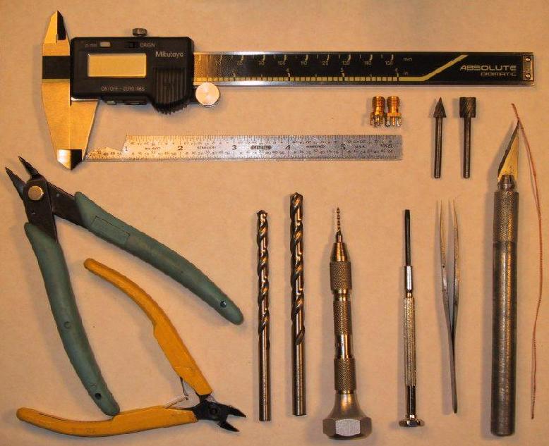
Equipment Required:
-------------------
You will _need_ the following items to successfuly modify this card.
Fine-Point soldering iron (you can't do with with what they sell at Radio shack. I love my METCAL. ;^) A weller may do the trick.)
Microscope (or other type of magnifier, or young, fresh eyes)
Solder Wick (a bulb will suck the solder and the components off the board.)
X-acto knife
Hotair gun (or nerves of steel, a blow-dryer will also work, but take longer)
Tweezers (very, very fine.. not the noze hair plucking variety)
Materials:
----------
Modification:
-------------
The first step is to cut an access hole into the bottom of the card to access both the RF connector PCB pad and the components that need to be removed and/or added. Arrows in the picture indicate where artifacts from the plastic injection process are located. One can use these artifact to cut a hole that will reveal the PCB mounting hole and SMC components. Layout the lines with a straight edge. Line up with the rectangular indentation mark and faint line for label placement.
The picture also shows the initial cut for the access hole. Perform a similar cut on your board. If you have trouble understanding the picture, refer to the text diagram below.
      \------------------+-------------------------------+
      /                  |                 ^             |
      \                  |                 |             |
      /                  |             22mm|.8650in      |
      \                  |                 |             |
      /                  |                 V             |
      \     main         |       ------------------      |
      \      PCMCIA      |     ->|                |      |<- 25.4mm
      /        body      |       |                |      |   1.00in
      \                  |       |                |      |
      /                  |       |              ->|      |<- 5.25mm
      \                  |       |                |      |   .158in
      /                  |       ------------------      |
      \                  |                 ^             |
      \                  |                 |             |
      /                  |             22mm|.8650in      |
      \                  |                 |             |
      /                  |                 V             |
      \------------------+-------------------------------+
Once the lines are drawn, score with the x-acto knife approximately forty times on each edge, slightly inwart. The removed plastic piece should be trapezodial in shape. Remove and save this material, we will use it to act as a covering once the modifcation is complete. Your card should now resemble this.
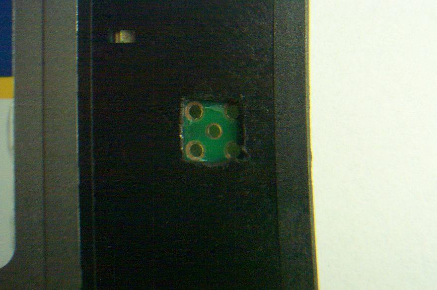
Now we must mark where the SMC threaded connector will protrude through the top side of the plastic cover. Mark the center in top lid with a drill bit through the center hole in the PCB pad. This picture illustrates the procedure. Once completed, turn the card over and it should appear as so.
If you look carefully at the top of the plastic area of the PCMCIA cover, you will realize that there is a sticky layer of plactic providing a cover for the LED to shine through. Remove the sticky cover and put aside for now. Your card should look like this.
Very carefully, drill/route a 5/16 hole using the center hole we drilled previously into the top plastic housing of the PCMCIA card. If you don't have access to a dremel tool or drill, you can use a bit larger than 5/16" and slowly twist in your fingers until you produce a 5/16" hole. NOTE: The drill or routing bit MUST BE FLAT, not pointed. You don't want to damage the PCB under the plastic housing. Completed, your card shold now look like this.
If you are going with the round base SMA connector, skip the next step.
If you are using the square base SMA connector, you will need to square the round hole. You can do this with a pair of dykes. Notch each corner and then square off with an X-acto knife. It's ok if there is a little slack around the connector base, as the sticky cover will cover it if you don't screw up drilling the hole in it.
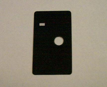
Now drill a 1/4" hole through the sticky cover using the center hole you previously drilled. You can make it slightly smaller than 1/4" for a snug fitting slick look. Your sticky cover should now look like this.
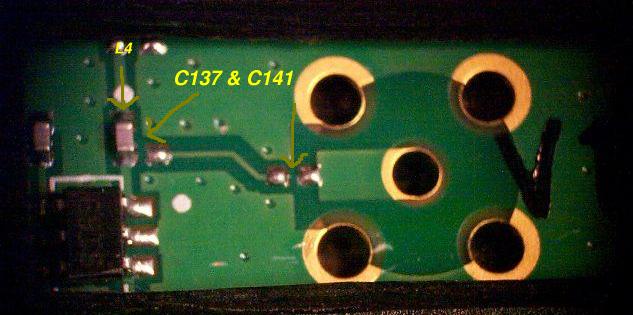
Locate L4, C137 and C141 on your card. They can be seen here. Remove inductor L4. Do this by placing the solder wick on one side of the inductor and applying heat on top of the wick where the inductor is underneath. It should only take a moment for the wick to "suck" up the solder. Perform the same action to the other side of L4 with greater care as the removal of the solder may result in your dragging your sharp, hot, soldering iron tip across the board, severing traces as you go. Once removed, wick away all excess solder from all of the pads, resembling this. NOTE: The connector is installed in this picture, however, we recommend that you do this AFTER you complete the component soldering.
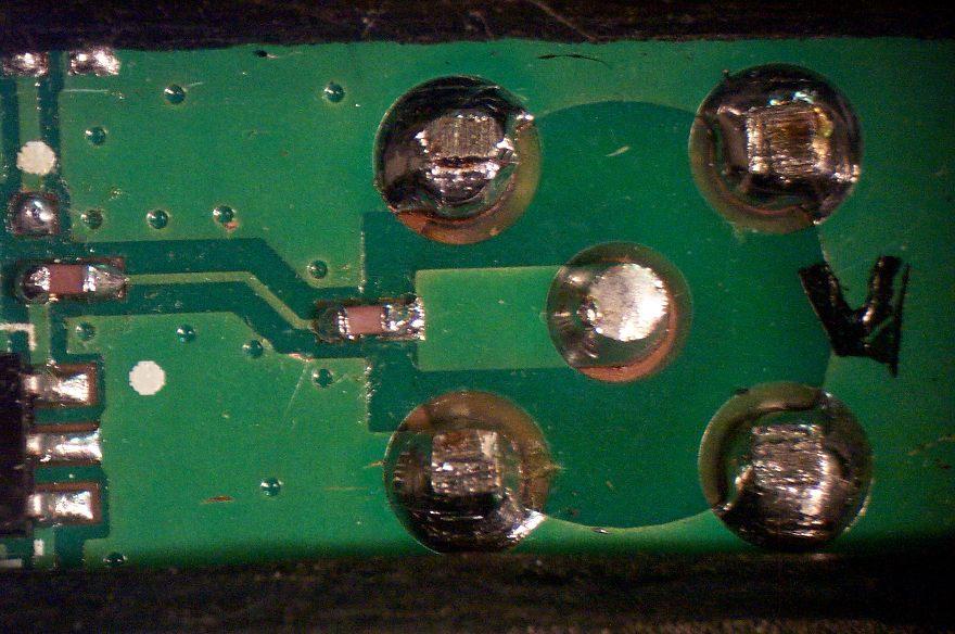
Next we install C137 and C141 with a 150pf capacitor. It would be best if you put a dab of solder on one of the pads before installing the capacitor. Then all you have to do is heat the solder back up, and using tweezers, move the capacitor into the molten solder, aligning it so that it rests on both pads, one end in the molten solder, and the other end on the vacant pad. Then heat up the pad and other end of the cap with the iron *gently* and just apply a slight amount of solder to it. It is very easy to create a ball of solder so be careful. After installation, your board should look like this. We are ready to finally install the RF connector.
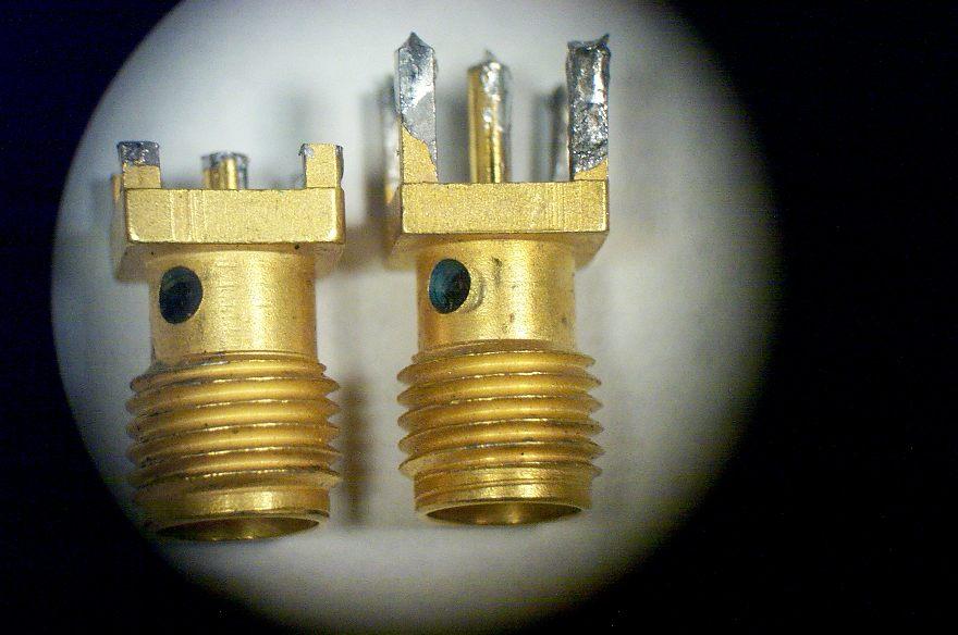
Before installing the PCB mount RF connector, the least of the connector must be trimmed PRIOR to installation. Trim the least on the connector to 1.5mm/3/32". This picture should help you visualize the length.
Install J1, the RF connector. Next, install the connector (either round or square, depending on the hole you prepared earlier) soldering all five leads after.
Re-Assembly:
------------
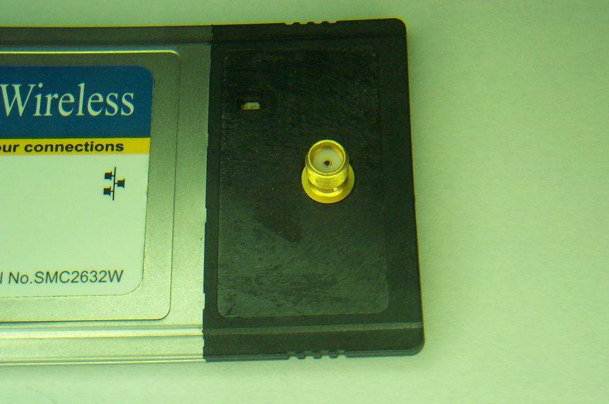
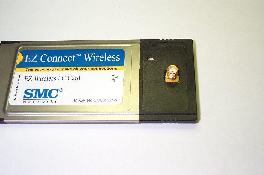
Now, all we do is drop on the sticky cover over the SMC connector (you may need to screw it down the thread if you cut the hole for the snug fitting slick look). Then take the trapezoid piece of plastic we removed earlier in the procedure and either glue or tape in place. Viola! Go and play..